We think in innovative solutions.
Leading edge plasma solutions
We develop and manufacture innovative and reliable solutions to meet the most stringent requirements and deliver advanced processing capabilities to our customers. Our solutions are designed to allow high volume manufacturing with the lowest Cost of Ownership. They are used by several top 10 IC manufacturers and top 10 packaging houses and includes many IDMs, OSATs, IDMs, and RTOs around the globe.
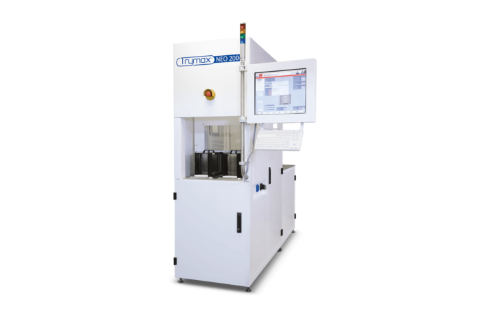
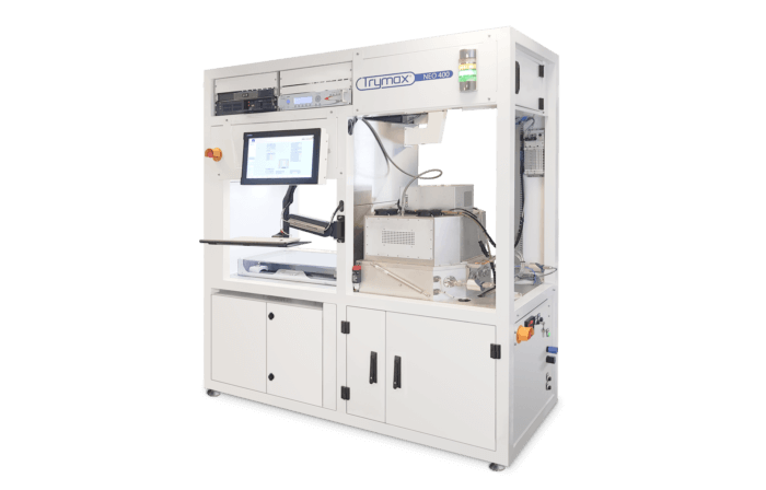
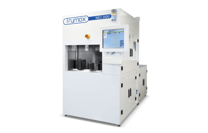
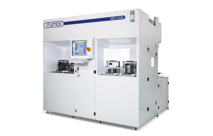
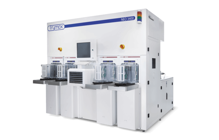
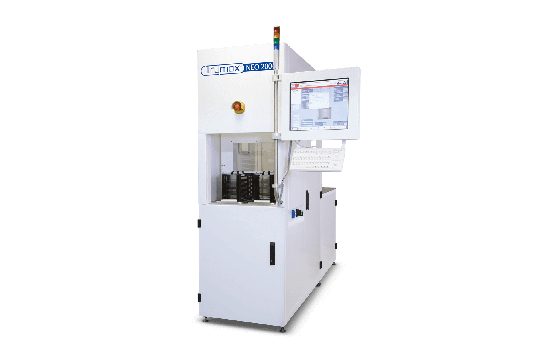
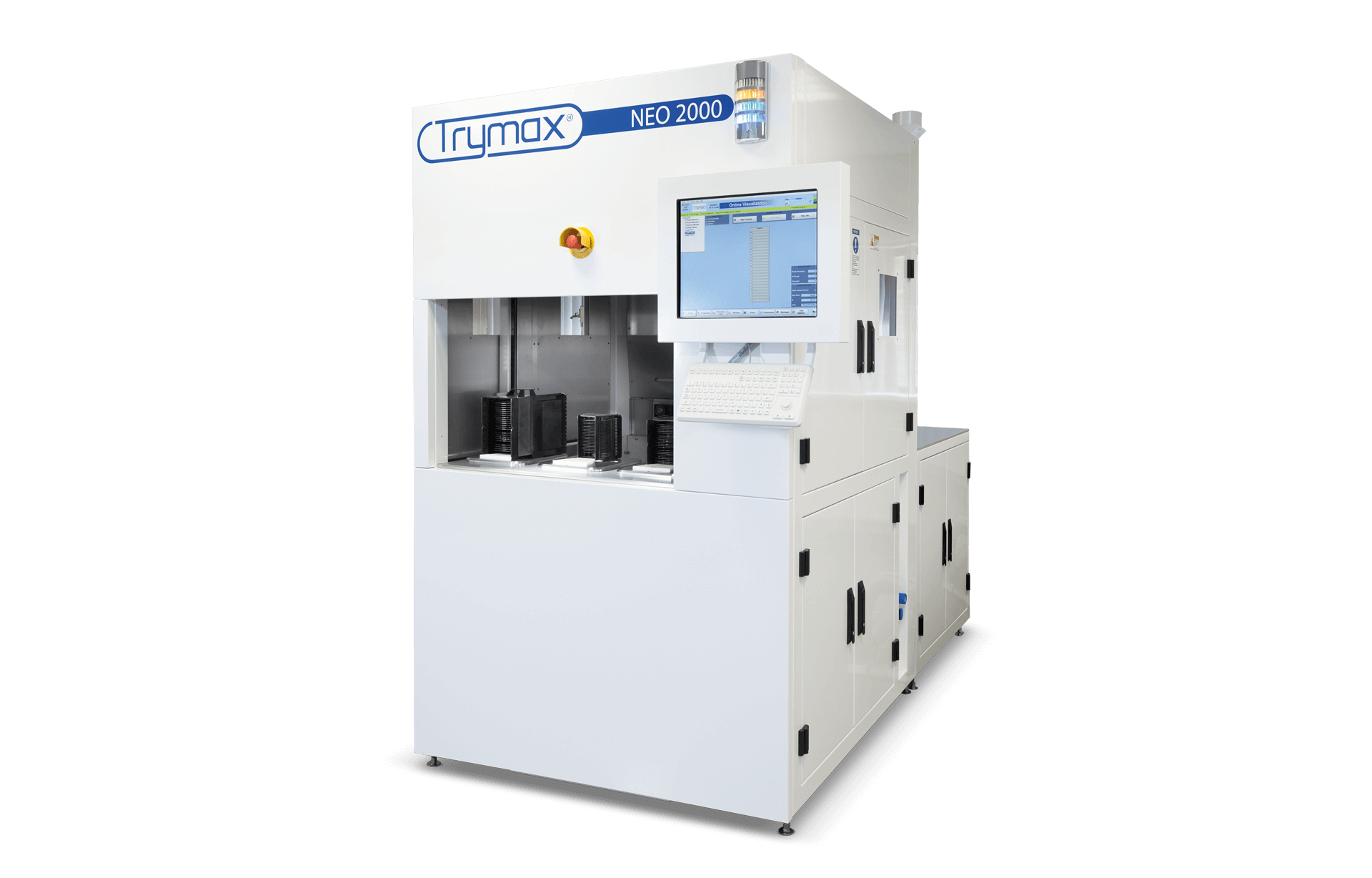
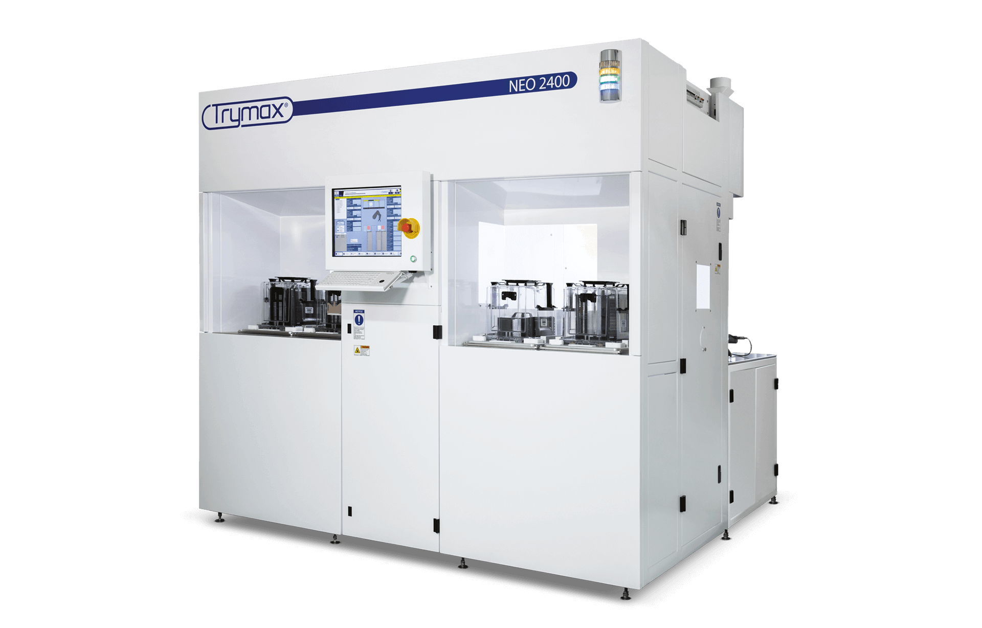
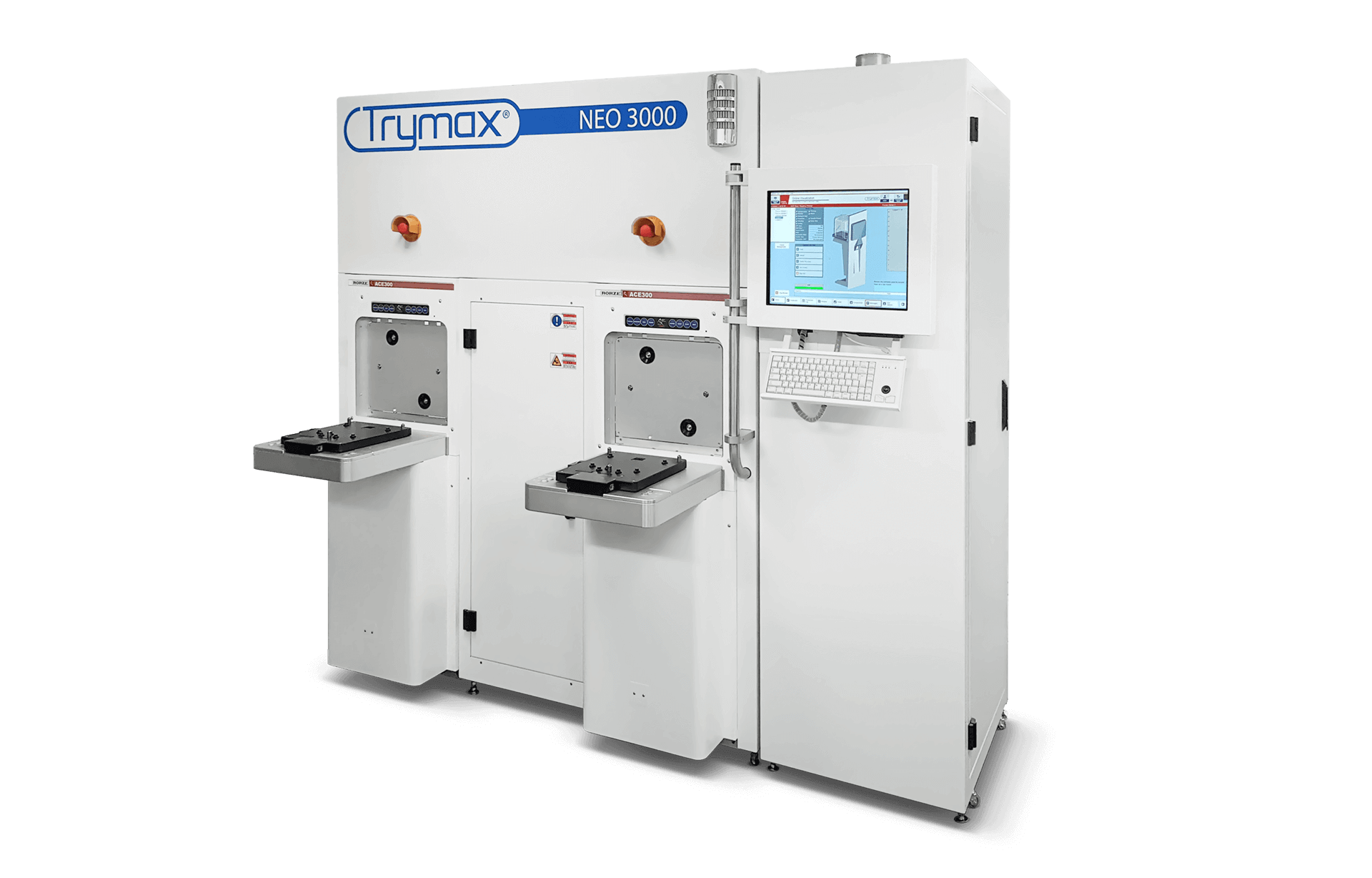
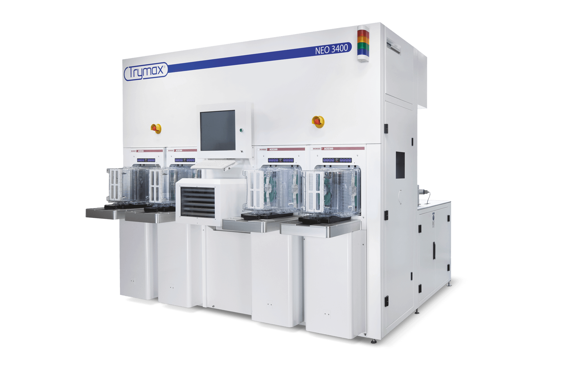
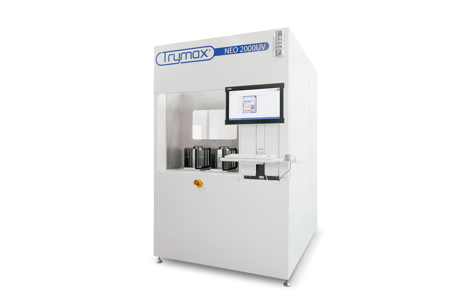
The Trymax NEO 200A, NEO 2000 and NEO 2400 product series can handle seamlessly multiple wafer sizes up to 200mm. The Trymax NEO 3000 and NEO 3400 product series can handle 300 and 200mm wafer sizes with true bridge capabilities. Our plasma solutions can be delivered with RF, microwave or dual source technologies and can be configured with 1, 2 or 4 process chambers depending on the customer requirements. Our NEO 2000UV solution is the latest addition to our portfolio and is dedicated to photoresist curing and charge erasing. It accommodates wafer sizes up to 200mm in a dual chamber configuration.
We innovate to deliver products and solutions
Our customers are using our equipment to address a wide range of applications during the semiconductor manufacturing process. Companies involved in CMOS, Power, RF, MEMS, LED, as well as Wafer Level Packaging can benefit from our solutions. Various types of materials, wafer sizes and thicknesses could be processed on our NEO series.
Learn more about Trymax Semiconductor Equipment.
Throughout the year, we will visit events around the globe. At the event you can visit our booth, pick up a brochure and ask our Trymax team your questions.